본 연구실인 Bit Engineering Laboratory(줄여서 BitE Lab)에서는 주로 디지털로 구현되는 system on a chip (SoC), 즉, 시스템 반도체를 연구합니다. 거의 모든 전자 장치는 초고밀도로 집적된 칩(chip)을 탑재하고 있고, 현대 전자 공학에서는 이 칩 위에 시스템 전체가 구현 되어있는 경우가 흔합니다. 통신, biomedical, 자동차, 스마트폰, 가전, 산업 제어/자동화, 로봇, 조선, 국방 등 응용 분야마다 시스템이 달라지겠지만, 기본적인 SoC 아키텍처는 크게 달라지지는 않는다고 말할 수 있습니다. 즉, 한 개 혹은 여러 개의 프로세서, 각종 메모리 (SRAM, DRAM, cache, flash/ROM 등), 각종 입출력 주변 장치 (I/O peripherals or IOP) (UART, Ethernet, I2C/SPI, USB, ADC/DAC, timer, GPIO) 등의 IP(intellectual properties)가 버스 및 interconnection network에 붙게 됩니다. 이 때 프로세서는 사용자가 C 언어 등으로 코딩한 소프트웨어를 실행해 주는 핵심 IP로서, SoC의 두뇌 역할을 하기 때문에 코어(core)라고도 불립니다. 그리고 뼈대 역할을 하는 것이 칩 상 버스(on-chip bus) 및 칩 상 네트워크(on-chip network 혹은 OCN)입니다. OCN이 들어간SoC를 특별히 network on a chip(NoC)이라고 합니다.
BitE Lab에서는 주어진 응용 분야에 맞는 SoC를 연구합니다. 이렇게 특정 목적에 부합하는 SoC를 임베디드 SoC라고 합니다.우리 랩에서 목표로 두고 있는 응용 분야는 크게 사물 인터넷 (Internet of things 혹은 IoT), 인공 지능(artificial intelligence 혹은 AI)을 위한 machine learning / 신경망(neural networks), IoT의 대표적인 통신 방식 중 하나인WLAN (일명 Wi-Fi) 등입니다.
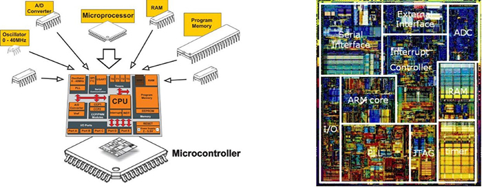
SoC는 기본적으로 소프트웨어(S/W)와 하드웨어(H/W)를 포함하고 있습니다. S/W를 실행시켜 주는 IP가 프로세서이고, 이는 마이크로프로세서, 마이크로컨트롤러 장치 (microcontroller unit 혹은 MCU), 디지털 신호 처리기 (digital signal processor 혹은 DSP) 등을 포함합니다. 좀 더 빠른 속도가 요구되는 기능(function)/동작(operation)은 전용(dedicated) H/W logic으로 구현하는 경우가 많습니다. 이러한 디지털 logic을 H/W 가속기(accelerator)나 glue logic이라고도 합니다. Very large scale integrated (VLSI) SoC의 처리 속도를 향상시키기 위해 쓰이는 대표적인 방법으로는 pipelining과 parallelism이 있습니다. 프로세서 코어를 동시에 두 개 이상 사용하여 코어마다S/W(thread)를 실행시키는 병렬 처리 기법을 multicore 기법이라고 부르는데, 넓게는 범용 그래픽 처리 장치(general purpose graphics processing unit 혹은 GPGPU)도 포함하게 됩니다. Multicore로 구성된 SoC를 multiprocessor SoC(MPSoC) 혹은 chip multiprocessor(CMP)라고도 부릅니다.
BitE Lab에서는 IoT, machine learning / 신경망, WLAN 등의 응용 분야를 위한 알고리듬을 상위 수준 언어의 S/W로 모델링 및 분석(profiling)하여, 응용 분야에 맞는 프로세서 H/W와 SoC/NoC를 설계 및 구현합니다. 각종 전자 공학 및 융복합 응용 분야의 관련 알고리듬이 달라져도, 이를 구현한 제품(commercialized products)이SoC/NoC 형태이고, 위에서 언급한 IP들로 구성된다는 기본적인 사실은 달라지지 않습니다. 따라서, 다양한 응용 분야를 S/W-H/W SoC/NoC로 구현하는 기술이 현대 첨단 공학 기술의 요체이자 정수입니다.
이른바 4차 산업 혁명 시대에 IoT와 머신 러닝 기반 인공 지능은 시너지 효과도 불러 올 것입니다. IoT 시스템은 크게 센서, 프로세서, 통신 모듈의 세 가지 성분으로 나누어 볼 수 있는데, 프로세서는 계산(연산)과 제어를 담당하고, 통신 모듈 중 WLAN은 IoT 무선 통신 방식의 대표적인 후보 중의 하나로서 가장 성숙되고 체계적으로 발전해 온 표준입니다. 이들을 묶어서 C3I라고 합니다. (즉, computation, control, and communication for IT) BitE Lab에서는 머신 러닝, IoT, WLAN용 SoC/NoC 및 customized processor/ASIP을 주요 연구 토픽으로 삼고 있습니다. 해당 응용 분야의 알고리듬을 먼저S/W로 만든 후, 응용 분야를 위한 프로세서를 만들고, OCN, 가속기, 메모리, IOP 등 여러 IP로 이루어진 SoC/NoC도 설계, 구현합니다.
- Low-end embedded microprocessors for IoT
- SoC/NoC based on customized processor cores and tailored to a specific application
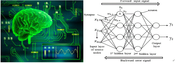
- Machine learning / neural network processor/SoC/NoC/accelerators
- Wi-Fi MAC SoC and MAC-PHY cross-layer integration

SoC의 S/W 설계는 주로 C 언어를 이용해 수행하고, 선행적으로 Matlab을 이용하기도 하며, 가능한 한 초기 단계에서 H/W-S/W partitioning을 하기 위해 TLM (transaction-level model) 모의실험을 하는 경우, SystemC를 이용합니다. SystemC는 일종의 C++ library라 할 수 있으므로 C++에 대한 지식이 있으면 도움이 됩니다. VLSI SoC의 H/W 설계는 RTL(register transfer level)에서(Verilog) HDL(H/W description language)을 갖고 수행하고, 구현(implementation)은 주로 보드 수준에서 수행하는데, 먼저 FPGA로 prototyping하고, 그 다음에 ASIC으로 갈 수 있습니다. ASIC 설계의 앞 단계(front-end)에서는 디지털 로직 게이트 수준의 모의실험(simulation) 및 합성(synthesis)을 수행하고, 뒷 단계(back-end)는 반도체 제조 회사(fab)로 넘겨 줄 설계 도면(layout)을 만들어 주는 단계로서 physical design을 의미합니다. FPGA 및 ASIC 설계 시 EDA tools의 도움을 받아 설계하고, 성능(performance)과 복잡도(complexity) 간의 trade-off(타협)를 분석합니다. BitE Lab에서는 위 flow에서도 가장 핵심적인 FPGA 수준 설계 및 ASIC front-end 설계를 주로 합니다. FPGA와 ASIC 모두 simulation용EDA tools 한두 종류, synthesis용 EDA tools 한두 종류를 이용해 설계할 수 있습니다. SoC의 S/W와 H/W는 동시 설계(co-design)를 진행하여 time to market (TTM)을 줄입니다. 설계된 시스템은 보드 수준에서 디버깅 및 검증을 수행합니다. BitE Lab에서는 고성능 Xilinx FPGA 칩이 탑재된 보드 및 programmable SoC(Xilinx Zynq)가 탑재된 보드 등을 사용합니다.
구체적으로 설계했거나 설계 중인 IP는 몇 종류의 마이크로프로세서, customized processor (ASIP), 몇 가지 메모리 컨트롤러, 인터럽트 컨트롤러, 타이머, 캐시, UART, 전용 H/W 로직, 버스 등입니다. 응용 분야 및 알고리듬을 고려한 컴퓨터 아키텍처, SoC 플랫폼 아키텍처, OCN/NoC 아키텍처 등도 연구합니다.
SoC/NoC및 프로세서의 주 관심 응용 분야는 IoT, machine learning / AI / neuromorphic technology (NMT or 인공 뇌 신경망 모방 기술) / Wi-Fi (IEEE 802.11 series WLAN) 등입니다. 이러한 분야는 산업 전반에 매우 광범위하게 적용되고 있고, 앞으로는 더 확대될 것입니다.

응용분야에 특화된 임베디드 SoC는 응용(application) S/W를 돌리기 위한 개발 환경이 필요한데,이를 toolchain이라 부르고, 컴파일러, 어셈블러, linker, loader, 디버거, archive library, ISS (instruction set simulator) 등을 포함하는 경우가 흔합니다. 고성능 SoC일 경우에는 system S/W의 하나인 OS를 쓰는 경우도 생깁니다.
Bite Lab은 SoC 설계를 위한 EDA tools(FPGA simulation & synthesis용tool, ASIC front-end simulation용 tool, ASIC front-end synthesis용 tool, 프로세서 설계 및 합성용tool 등)를 사용하고 있습니다. 보드 수준 emulation은 고성능 FPGA 칩 탑재 보드, programmable SoC 탑재 보드 등에서 수행하고 있습니다. EDA tools를 써서 on-chip 테스트, 디버깅을 주로 하지만, 필요할 경우 오실로스코프, 로직 분석기 등을 사용할 수도 있습니다.

본 연구실에서 연구했거나 연구 개발 중인 응용 분야는 다음과 같이 요약할 수 있습니다.
1. IoT 관련 응용 분야를 위한 (목적에 부합하는) SoC 및 low-end 임베디드 프로세서
2. 응용 분야에 특화된 임베디드 프로세서 코어 (customized processor or ASIP) 기반의 SoC/NoC/MPSoC
3. 머신 러닝용 S/W-H/W SoC/NoC
4. WLAN SoC 및 MAC-PHY cross-layer integration
이에 대한 부가적인 설명은 다음과 같습니다.
1. IoT 관련 응용 분야를 위한 (목적에 부합하는) SoC 및 low-end 임베디드 프로세서
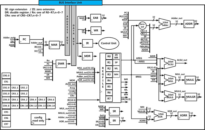
BitE Lab에서는 IoT를 위한 low-end 임베디드 프로세서 코어를 설계했습니다. 시스템의 두뇌 역할을 하는 프로세서는 크게 datapath와 control unit으로 나눌 수 있는데, datapath는 각종 computation을 실행하고, 대부분 FSM 타입으로 설계하는 control unit은 컨트롤러(제어기) 역할을 맡고 있습니다. BitE Lab에서는 2013년부터 2015년까지 low-gate-count, low-complexity, low-power, high-code-density 4-bit multicycle 프로세서, 16-bit multicycle 프로세서, 32-bit 5단 파이프라인 프로세서, 32-bit 2/3단 파이프라인 프로세서 및 이를 위한SoC 등을 개발했습니다. 이 중 32-bit 2/3단 파이프라인 프로세서는 아두이노 경량 우노 보드에 탑재돼 smart metering 등의 IoT용으로 쓰이고 있습니다.
프로세서 설계는 ISA(instruction set architecture)를 기초로 하여 이루어지고, RTL flow를 작성한 후 CPU(central processing unit, 즉 중앙 처리 장치)의 datapath와 control unit을 (Verilog) HDL로 설계합니다. 제어기는 명령어 해독, 해저드 처리, 인터럽트 및 예외 처리 등을 수행합니다. 이렇게 1차 설계된 프로세서는 테스트 벤치 모의실험과 보드 수준 검증을 거쳐 refine되고, 컴파일러를 이용한 S/W-H/W 통합 검증 및 벤치마킹 테스트도 거칩니다. H/W는 FPGA에서 prototyping 하고, EDA tools를 써서 ASIC front-end 합성 후 성능-복잡도 trade-off를 분석합니다.
2. 응용 분야에 특화된 임베디드 프로세서 코어 (customized processor or ASIP) 기반의 SoC/NoC/MPSoC
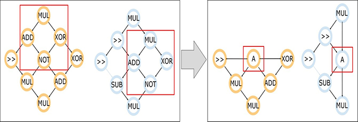
맞춤형 임베디드 프로세서에도 관심을 갖고 있습니다.특정 응용 분야를 위한 프로세서는 특정 하드웨어를 추가적으로 갖거나, 특별한 명령어들을 기반으로 만들어질 수 있습니다. 이러한 application-specific instruction-set processor, 즉, ASIP를 위해서는 대개 해당 응용 분야의 알고리듬/function/behavior를 상위 수준에서 모델링/모의실험/분석(profiling) 한 후 이로부터 ISA를 정의/선택/확장/합성합니다. 동일한 알고리듬을 구성하는 여러 개의 명령어를 하나의 새로운 명령어로 생성하는 명령어 확장 기법 등을 적용할 수 있습니다. 이런 방식으로 추출된 ISA에 기반을 두고, 메모리/레지스터 접근, 속도 성능 등의 cost function을 최적화하는 ASIP를 만들 수 있습니다.
BitE Lab에서는 프로세서 외에도 버스, OCN을 비롯하여, 캐시 메모리, 주 메모리, 각종 IOP, co-processor / 가속기 / 전용 로직, DMA 컨트롤러IP 등에도 관심을 갖고 있습니다. S/W 설계 시에는toolchain 개발 환경을 써서 C/C++ 등을 컴파일, profiling 및 디버깅 하는 반면에, H/W 설계 시에는 (Verilog) HDL을 쓰고, EDA tools로 simulation 및 synthesis(합성)를 수행합니다. S/W-H/W 통합 검증 시에는 컴파일 된 결과를 프로그램 메모리에 올려 on-chip debugger (OCD) 등으로 검증합니다. 설계한 SoC 전체를 보드 상의FPGA 칩에 다운로드 하여 완성할 수도 있고, 상용 프로그래머블 SoC(Zynq 칩 등)를 활용할 수도 있습니다. FPGA prototyping 뿐만 아니라, ASIC front-end 합성 후 성능-복잡도 분석도 수행해야 합니다. 경우에 따라서는ASIC backend (physical design)까지 고려해야 하는 경우도 있을 것입니다.

3. 머신 러닝용 S/W-H/W SoC/NoC
대략 2013년 이후부터 더욱 증가 추세인 머신 러닝 관련 연구는 IoT 관련 연구와 함께 향후 4차 산업 혁명을 실현하기 위한 주요 연구 분야가 될 것입니다. BitE Lab에서는 CNN (convolutional neural network) 등의 신경망이나 SVM (support vector machine) 같은 머신 러닝 알고리듬을 위한 전용 프로세서, 인공 뇌 신경망 모방 기술 (neuromorphic technology or NMT) 등의 지능형 시스템 반도체에 관심을 갖고 있습니다. 딥 러닝용 CPU나 뇌 신경 모방 칩 연구 개발은 주요 R&D 토픽 중 하나입니다. Bite Lab에서는 머신 러닝 알고리듬을 위한 customized processor / ASIP, 그리고 다양한 방식의 머신 러닝용 SoC/NoC 구현에 관심을 갖고 있습니다.
4. WLAN SoC 및 MAC-PHY cross-layer integration
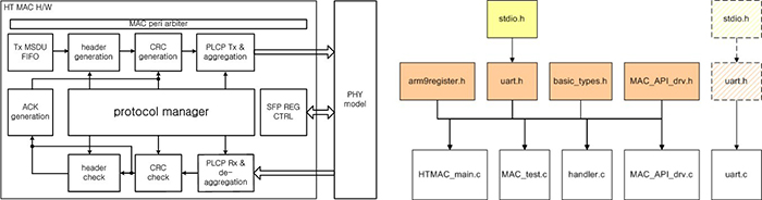
Bite Lab에서는 IEEE 802.11 series Wi-Fi MAC(medium access control 혹은 매체 접속 제어)를 위한 SoC도 개발하고 있습니다. S/W는 제어 용으로 주로 필요하고, 랩에서 직접 설계, 개발한 프로세서나 ARM 프로세서 등을 이용하여 돌리고, H/W는 헤더 (header) 생성/검사, 오류 제어용 CRC (cyclic redundancy check, 즉, 순환 중복 검사) 코드 생성/검사, frame aggregation/de-aggregation, ACK (acknowledgment) frame 생성, 전송 프로토콜 관리 등을 수행합니다. MAC SoC는 IEEE 802.11 표준 스펙에 나온 속도(throughput or bit rate)/지연 시간(latency) 요구 조건을 만족시켜야 합니다. Link adaptation은 채널 상태에 따라 전송 방식(변조 및 코딩 기법, 안테나 수 등)을 적응적으로 바꾸는 기법으로서, 대표적인 MAC-PHY cross-layer 기술입니다. BitE Lab에서는 Wi-Fi MAC에 PHY를 통합하여 link adaptation 등을 구현하는 일에도 관심이 있습니다. Link adaptation에도 machine learning이 쓰일 수 있습니다.